Dc Sputtering Ito
Composition of 9010 respectively. It is a simple technique when processing large quantities.
Magnetron Sputtering Deposition Technology Shanghai China Shanghai Royal Technology Inc
The power source is the Direct Current DC type.
Dc sputtering ito. Since the optimum characteristics in terms of resistivity for grown films were obtained at this substrate temperature it was chosen d d. Labnetwork DC sputtering of ITO Messages sorted by. Today there is strong need for the high-quality ITO films for different applications should be deposited at substrate such as polyethylene terephthalate PET 11.
Chamber pressure is usually from 1 to 100 mTorr DC power is usually preferred for electrically conductive target materials as its effective and economical. Annealing experiments have been done in vacuum and in Ar atmosphere up to a temperature of 450 C. Indium Tin Oxide ITO DC-magnetron sputtering.
Date thread subject author Sputtering at lower power will produce less heat and thermal stress and can delay flaking but flakes will still show up when the film deposited on your sputter. Amount of material added to a wafer. To test the advantages of mid frequency MF sputtering eg.
10172013 The Ag layers were deposited by DC magnetron sputtering with a power density of 173 Wcm 2 while the ITO coatings were deposited by radio frequency magnetron sputtering with a power density of 212 Wcm 2. Such coatings can be deposited either in a purely reactive sputter process from metallic In-Sn alloy targets or from ceramic ITO targets using a quasi-reactive process. 542021 In this context DC magnetron co-sputtering mechanism was utilized for the deposition of MoS 2 ITO and MoS 2 ITO composite thin films on Si substrate.
2 Deposited indium tin oxide ITO thin films by dc-magnetron sputtering 731 ITO films on plastic substrates by sputtering has been reported 9 10. 641998 Transparent heatreflective films consisting of ITOAgITO or ZnOAgZnO were deposited onto sodalime glass by dc magnetron sputtering. The intensity of this peak varies slightly according to the sputtering conditions.
Techniques for ITO thin film production sputtering is the most widely investigated and large-scale deposition setups are available 7-8 13. 9182014 Optimized DC magnetron sputtering system for the deposition of transparent conductive oxides TCOs such indium tin oxide ITO on glass substrate has been applied in order to achieve low-emitting low-e transparent coatings. ITO ultrathin films were deposited in reactive atmosphere using In 2O3SnO 2 composition of.
They are characterized with a broad peak between 30. DC sputtering a comparison of. Deposition techniques for ITO include DC and RF sputtering evaporation chemical vapor deposition and a number of high temperature deposition techniques involving spray or dip processing.
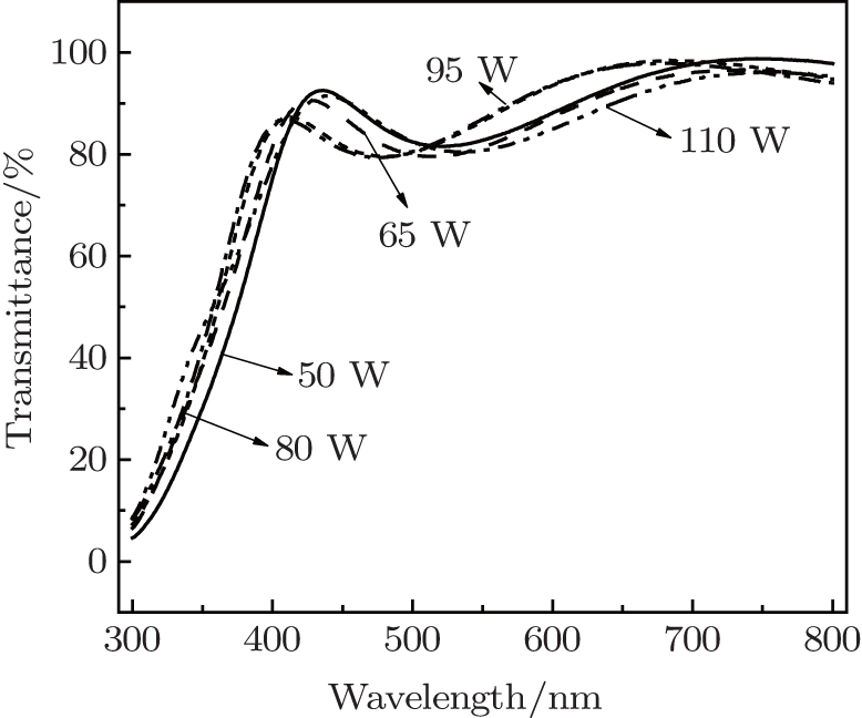
A change of texture from h100ito h111ias the ppo. Ceramic ITO targets of In 2 O 3SnO 2 disk 9010 wt 4N and an Ag metal target 4N were used for ITO and Ag layer deposition separately. To obtain the concerned electrical resistance and high infrared reflection first the effect of applied sputtering power then oxygen flow on the.
6 7 8 vs. We chose to deposit ITO films by the dc-magnetron sputtering method because a high sputtering rate and good film performances and low cost deposition system could be achieved comparing with a rf. Of 2Θ diffraction angle.
The structural electrical and optical properties of the ITO. These vaporized atoms are then deposited when they condense as a thin film on the substrate to be coated. Sputtering was chosen for this investigation due to the ability to carefully control the stoichiometry of the film by controlling film.
X-ray diffraction confirmed the hexagonal structure for MoS 2 and body centered cubic structure for ITO. The DC sputtering technique is used to deposit ITO TiO 2 and NTO transparent thin films on both glass and PET substrates with identical conditions. 3Sn ITO thin lms prepared by DC sputtering at di erent partial pressure of oxygen ppo.
The transmittance in the visible range of the ITOAgITO film was more than 80 and the reflectance at 10 μm was nearly. In particular the oxide layers were deposited from an electrically conductive oxide target. And dc sputtered ITO thin films with thicknesses of 40 and 70nm grown at a substrate temperature of 350 C.
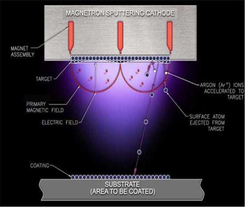
8301999 The properties of ITO films sputtered with the ceramic oxide target result in lower resistivities and the sputter technology is less complicated. 11262016 DC or Direct Current Sputtering is a Thin Film Physical Vapor Deposition PVD Coating technique where a target material to be used as the coating is bombarded with ionized gas molecules causing atoms to be Sputtered off into the plasma. 6152006 ITO films deposited by DC magnetron sputtering at room temperature show amorphous patterns regardless of the process condition as seen from the XRD data Fig.
ITO or tin-doped indium-oxide coatings have excellent electrical conductivity and optical transparency and are therefore used as transparent electrodes in most display products. We report on the study of the characteristics of indiumtin oxide ITO films prepared by well-controlled and reproducible DC magnetron sputtering in argon with consequent annealing in oxygen atmosphere.
Indium Tin Oxide Films Obtained By Dc Magnetron Sputtering For Improved Si Heterojunction Solar Cell Applications Xref Ref Type Fn Rid Cpb142922fn1 Xref

Target Poisoning Target Poison Eyeshadow
![]()
Transmission Spectra Of Ito Layers Deposited By Dc A And Rf B Download Scientific Diagram

Magnetron Sputtering An Overview Sciencedirect Topics

Pdf Optimization Of Sputtering Parameters For The Deposition Of Low Resistivity Indium Tin Oxide Thin Films
Komentar
Posting Komentar